Having a thorough understanding of the intricate components and processes that keep electronic devices and smartphones functioning is crucial. Among these components, the motherboard’s boot circuit is one of the most vital as it powers up your device and initiates its operations. To shed light on this crucial aspect, we aim to provide an in-depth analysis of the motherboard’s boot circuit, including its components and stages of operation.
The Key Components of the Boot Circuit
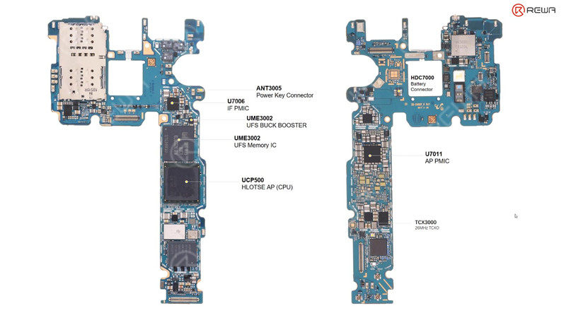
To comprehend the boot circuit fully, we must first familiarize ourselves with its essential components:
1. Battery Connector: This connector serves as the vital link between the battery and the motherboard, providing the initial power source. Its role is pivotal in the boot process.
2. IF PMIC (Power Management Integrated Circuit): The second component is the IF PMIC, which primarily supplies VBAT power to the AP PMIC USF Buck boost IC and the power on related contacts.
3. Power Key Contact: These contacts are integral to the power-on process, and pressing the power button triggers them.
4. AP PMIC (Application Processor Power Management Integrated Circuit): This component supplies power to the CPU and controls the entire boot process.
5. CPU (Central Processing Unit): The CPU, often represented as UCP500, governs the boot process, communicating with the UFS to extract boot programs and operating system information.
6. UFS Memory IC: This chip stores boot programs and the operating system, making it a crucial element of the boot circuit.
7. UFS Buck Boost IC: Responsible for providing power to the UFS Memory IC, this tiny chip plays a significant role in the circuit.
8. Crystal TCX3000: This crystal provides the necessary frequency for both the CPU and IF PMIC, ensuring synchronization in the boot process.
Now that we’ve identified the key players, let’s dive into the working stages of the boot circuit.
Working Stages of the Boot Circuit
The boot circuit’s functionality unfolds in several distinct stages:
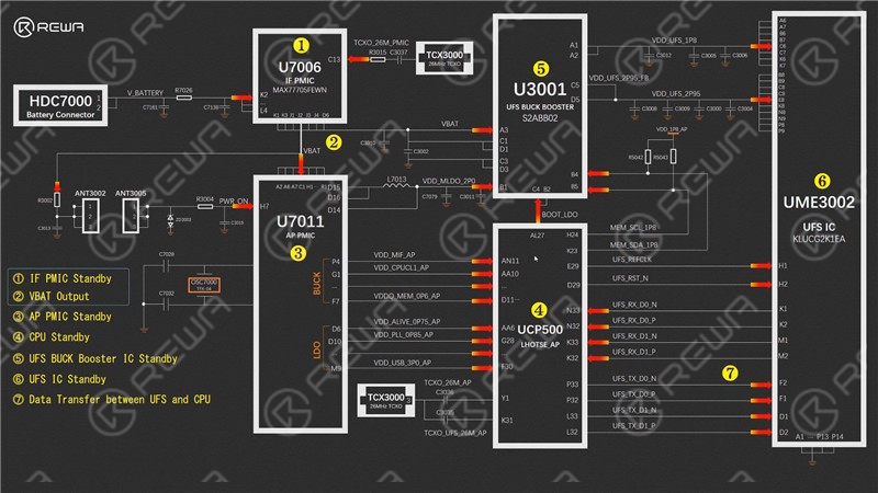
1. IF PMIC Standby: IF PMIC should be in standby mode for the first stage, with standby conditions including power and frequency from the crystal. Power is supplied by the battery, specifically the V_BATTERY. Once passing through the resistor, it will be directed to the IF PMIC, while the crystal will provide the working frequency for the IF PMIC.
2. IF PMIC Power Distribution: Once two conditions are met, this particular component will be ready for operation. The subsequent step involves supplying VBAT to various chips. The VBAT is divided into three main branches: one is directed towards the buck-boost IC, another is routed to the AP PMIC. Additionally, as previously mentioned, the third branch is connected to this contact, which primarily relates to the power-on trigger signal. It is worth noting that the voltage values of these two conditions, V_BATTERY and VBAT, can be measured prior to pressing the power button.
3. AP PMIC Standby: First, let’s move on to the third stage, which involves the standby operation of the AP PMIC chip. The working conditions for this chip are similar to the previous stage. Firstly, it needs to be powered. In this case, the VBAT is directly supplied to the chip. Secondly, there is a power-on signal. Before pressing the power key button, the voltage on one of the contacts is 0 volts. However, once the power key button is pressed, these two contacts will be connected, causing the voltage to be pulled up to the VBAT level.
4. CPU Standby: Once the power key button is pressed, hold it for a few seconds before releasing it. This action will cause the voltage to drop to 0 volts. Therefore, the process of pressing the power key button results in a change in voltage. In addition to this, the power key button generates the PWR_ON signal, and the crystal provides the necessary working frequency for the AP PMIC. Once power, PWR_ON, and the frequency requirements are met, the AP PMIC enters standby mode and the CPU is also ready to work in the fourth stage.
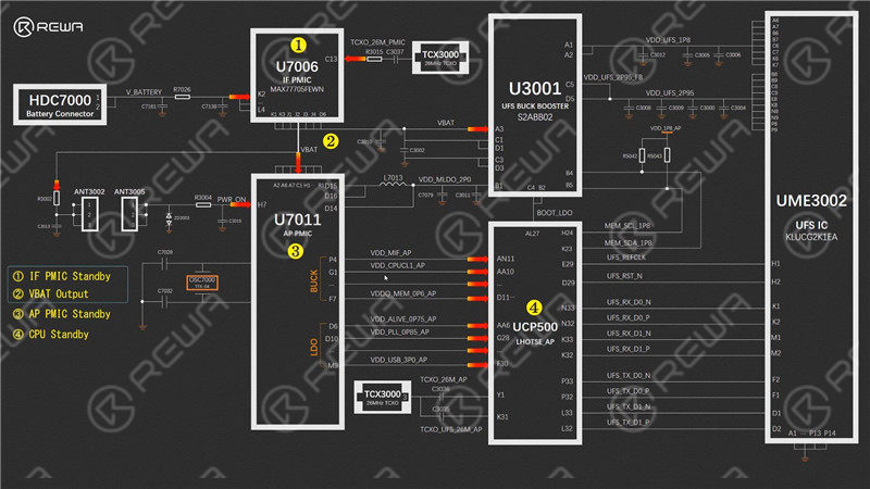
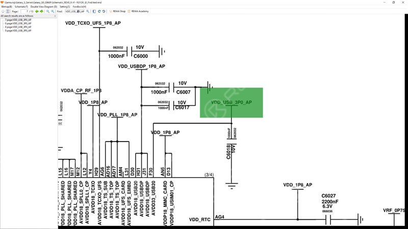
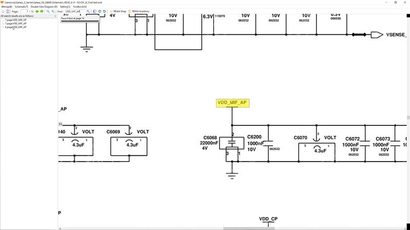
5. UFS Buck Boost IC Standby: Working conditions are also identical. The primary powers always come first. BUCK powers and LDO powers are observed to be generated from the AP PMIC and supplied to the CPU. Due to limited space, some power rails are not visible here. To examine the remaining power rails and their associated components, refer to the schematic for detailed information. For instance, let’s search for VDD_MIF_AP. It originates from the AP PMIC, U7011, and is supplied to the CPU. The CPU pins are shown here, along with the connected components related to this rail. Once the power supply is established, this crystal will provide the CPU’s frequency.
6. UFS IC Standby: Once the CPU is adequately powered and operating at the desired frequency, it becomes ready to execute its tasks. Similarly, the UFS buck boost IC also needs to be prepared for operation. As previously stated, the buck boost IC has two power sources: VABT and VDD_MLDO_2P0. Additionally, the CPU sends a BOOT_LDO signal to the buck boost IC. Moreover, the CPU manages the UFS buck boost IC through the I2C Bus, which includes pull-up resistors on the corresponding rails and utilizes the SCL and SDA signals. Once the power, BOOT_LDO signal, and I2C control signal are established, the UFS buck boost IC is set for operation.
7. Data Transmission: The final step involves transmitting data between the UFS and CPU, as previously mentioned. Boot programs or operating system information is exchanged between the CPU and UFS IC. Notably, the signal direction differs: one is for reception, while the other is for transmission. This describes the functioning of the boot circuit.
Conclusion
Understanding the intricate workings of the motherboard’s boot circuit is essential for anyone dealing with electronic devices. This comprehensive guide has shed light on its critical components and the stages of its operation. Armed with this knowledge, you can appreciate the complexity that goes into powering up your smartphone or other electronic gadgets.
For more in-depth information and courses on Android and electronics, consider visiting REWA Academy.
By grasping the fundamentals of the boot circuit, you’re better equipped to troubleshoot issues, optimize performance, and appreciate the marvel of modern technology. Whether you’re a tech enthusiast or a professional, this knowledge is a valuable asset in today’s digital age.
